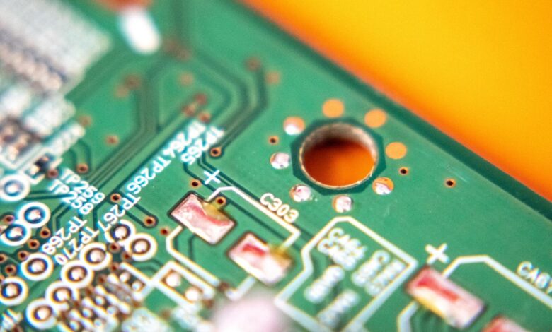
Microvia PCB
Microvias are defined as holes drilled into a PCB with a 1:1 aspect ratio and a depth of 0.010 inches. If a via’s diameter was 0.006 inches or less, it was previously classified as a microvia by the IPC. However, because of advances in laser technology, such precise drilling is now routine.
The IPC has settled on a new microvia definition based on a 1:1 aspect ratio and a depth threshold of 0.010 inches. PCB layers can be connected by microvias, also known as uVias. They rarely link more than two levels consecutively.
Varieties of Microvias
PCB designers can drill a wide variety of microvias. In terms of aspect ratio, microvia of all varieties are identical in size. Their relative positioning is the fundamental distinction between them.

- Boreholes called blind microvias are drilled to provide access from the outside to a deeper stratum. These holes are drilled into the PCB from the side rather than through it.
- Buried Microvias are vias drilled deep within a PCB’s inner layers but do not connect to the board’s exterior.
- Multiple blind or buried microvias are piled on top of one another to provide access to the internal layers.
- Microvias that are buried at varying depths are said to be staggered. There is no layering or stacking of these microvia. These are separated from one another instead.
- Microvias with holes drilled directly into the copper solder pad of the component are called via-in-pad microvias. Using this method, PCBs can be made smaller.
The use of microvias PCB in printed circuit board design has the potential to provide numerous advantages to the PCB designer. The functionality and performance of the board are improved by the thermo-mechanical reliability provided by microvias. The capability to manufacture via-in-pad microvias enables the downsizing of circuit boards, which is necessary as they shrink and lighten to fit into mobile devices. Given that they are smaller than a typical via or plated through hole, microvias provide more room on the circuit board. The smaller the boards, the more components can be attached to them without the need for larger boards.
PCB Via and Pad Size Basics
The size of the microvia PCB pad on the surface layers, where traces land to make electrical contact, is an open subject. There are a few locations to check while deciding on the land size for a via:
The Price of Production
A larger through will result in cheaper production costs. Vias of a greater size will necessitate correspondingly larger pad dimensions.
Width of Traces
Pads should be somewhat bigger than vias. Therefore, a larger pad size is required for use with a wide trace width, such as a wide controlled impedance trace.
Reliability
Larger areas are more reliable. IPC standards provide extensive guidance and will be used to establish whether or not a certain drill strike results in a via-pad problem.
Layer Count and Layer Type
Once the layer count exceeds 8 layers, pad size will also be affected by the layer count/
PCB Via Size and Pad Size Guidelines
Some concerns in PCB design and layout may appear elementary, but their answers are actually complex and connected to a wide range of critical manufacturing issues. The compatibility between microvia PCB through size and pad size is one such design element.
A landing pad is required for every microvia PCB and serves as a place to park traces when they are routed into the pad. While a well-matched pad and via size is a crucial parts of reliability, there are specific standards that must be followed.
Another critical design feature encountered in production is known as annular rings, and their selection is related to the size of the pads you select. According to IPC requirements, microvia PCB lands must be sized so that the annular ring created during production is large enough to accommodate the layer count.
- Size Pads Based on Annular Rings
There are additional PCB designs, such as flex boards or HDI boards, for which we employ alternative annular ring standards for size-based calculations. The terms annular ring, land, and pad are used interchangeably by certain designers.
An annular ring can mean how far anything is drilled before it reaches the pad’s outermost or innermost layer. The board will undergo drilling after the etching stage of PCB production. A CNC drill may not precisely center itself in the microvia PCB pad due to drift.
This means there will be a small amount of the annular ring remaining. Therefore, the pad size of your vias should be at least big enough to allow for any drill wander and still leave enough copper leftover to guarantee that the bare minimum annular ring is accommodated without causing a problem. Microvia PCB can be considered defective, and the board discarded if they fall beyond the tolerances.
- Microvia Aspect Ratio
As PCB designs shrink and get dense, we are also always on the hunt for new technology advancements that will make our jobs easier and allow us to achieve more. The microvia PCB is one of the advancements that can ease up the task for us. The laser-drilled vias vary in size and aspect ratio from standard vias. They reduce the complexity of routing traces and let you fit more routing into a given area.
Microvias differ from ordinary vias as they are drilled with a laser, which allows them to be smaller than a regularly drilled hole. They begin at a size comparable to a hole drilled by hand, typically no smaller than 0.006 inches, depending on the width of the board. Another distinction with microvias is that they normally only span two layers, as plating the copper inside these small holes can be problematic for fabricators. Microvias can be stacked on top of one another to allow for direct connections via multiple layers.
Surface-level microvias need not be filled, but subterranean microvias will be filled with materials that best suit the intended use. Electroplated copper is commonly used to fill stacked microvias and create interconnectivity between them. Another approach to linking microvias through the layer stack is to stagger them and connect them with short traces. A microvia has a different profile than a conventional via, resulting in a different aspect ratio.
Select the Right Microvia Aspect Ratio in Your HDI PCB
It’s natural for someone unfamiliar with printed circuit board design or electronics to be perplexed by the ever-shrinking form factors of today’s cutting-edge gadgets. You will see the development of HDI design for compact electronics with a high density of components, such as smartphones and small form factor embedded systems.
In multi-layer printed circuit boards, vias play a pivotal role in facilitating the routing of connections between signal layers and the power and ground planes. Careful planning of microvia PCB is required in an HDI PCB layout to guarantee reliability and conformity with manufacturing capabilities.
With the trend toward thinner and denser circuit boards, microvia PCB may seem like an attractive option for establishing the necessary connectivity in cutting-edge gadgets. When designing and routing with microvias, it is crucial to choose an appropriate microvia aspect ratio, as this is a key factor in ensuring reliability and facilitating manufacturing.
Fabrication of Microvias
Resin-coated copper foil and glass-reinforced epoxy are two examples of common PCB dielectrics that can accommodate microvias. Mechanical drilling and laser drilling are also viable options for making them for smaller aspect ratios.
Microvia PCB typically takes the following forms:
Unguided Microvia PCB
These microvias reach all the way from the topmost layer of an HDI stack to the bottommost. Structures like these can be left unfilled or filled with copper to facilitate soldering; however, microvia-in-pad designs should always utilize filled structures.
Blind Vias
Microvias that have been buried are essentially blind vias that are only allowed to exist in the interior layers. To ensure dependability and producibility, they must also adhere to the conventional aspect ratio standards. The correct procedure must be used to fill them to ensure that buried vias can survive the stress of reflow or thermal cycling.

Skipped Microvias
Unlike conventional microvias, which require multiple operations to create, skipped microvias only require a single step. In order to create the needed connection while keeping the required low microvia aspect ratio, these microvias are ideally employed to span across thinner dielectrics.
Laser-drilled Via-in-pad Technology in Your Microvia PCB
Drilling mechanically allows for microvias of greater diameters to be drilled without limiting the achievable aspect ratios. Since it is already used to install through-hole vias, it can be advantageous when the dielectric thickness is greater. However, on more substantial dielectrics, the bending of a thin drill during manufacture could lead to mis-registration. Remember that the greater the dielectric thickness, the fewer drill hits a mechanical drill can withstand. Therefore, you use a thinner dielectric when working with drilled microvias.
Microvias of smaller diameters can be fabricated by laser drilling; however, due to the laser’s limited depth of focus, the microvia PCB can only traverse a single layer of a thinner dielectric. Depending on the drill depth and the diameter of the via hole, these vias often have an aspect ratio that is less than 1. Multiple laser impacts may reduce the risk of misregistration compared to mechanical drilling, especially for longer stacked structures.
In order to raise the aspect ratio of the microvia or the reliability of the board, it is not possible to simply switch to thicker copper, at least for internally buried microvias. This is becausethe surrounding layer may not completely fill spaces around the edge of the microvia during pressing.
Spread glass weaves is a type of very dense fiberglass weave. The resin content will be low enough that there may be voids left over in the landscape. This is crucial because fiber weaving effects may become significant at greater speeds.
Laser-drilling Microvia for Via-in-pad Design
Multilayer PCBs necessitate vias; therefore, designers must plan for where to insert them before production can begin. The aspect ratio of mechanically drilled vias is higher, but the smallest diameter that can be drilled will be smaller. When the diameter of the vias is tiny, laser drilling becomes necessary. The same holds true for pads with via-in-pad layout.
Vias are an essential aspect of the escape strategy when working with high pin density components, such as BGA pad. Via-in-pad design is a need when the BGA pitch gets really narrow. When the diameter of a BGA pad is less than 0.5 mm, laser drilling is required to create microvias since conventional mechanical drilling would be too inefficient.
Because of its high precision and low access requirements, laser drilling is ideally suited for blind and buried vias. Since through-hole vias in multi-layer PCBs have to be drilled to such a depth that the resulting structures have a good aspect ratio, this process is almost often performed mechanically. But by layering blind or buried vias, designers can make a structure that goes through several layers while still being laser drillable.
Note that each segment of a stacked via structure introduces a new inductive discontinuity if you choose to utilize laser-drilled vias for better access to the internal layers of microvia PCBs rather than using mechanically drilled through-hole via. This can cause issues with signal reflection and resonance at the interface between the several levels of a stacked microvia.
If the impedance of the stacked vias is not properly matched, some signal frequencies will reverberate, causing excessive electromagnetic interference. Signal routing over shorter distances can benefit from the usage of stacked microvia PCB.
Cost Tradeoffs in Mechanical Drilling vs. Laser Drilling Microvia
PCB manufacturing costs become crucial in moderate to high-volume production runs. A few more cents each board can add up to a significant sum over time. The constant and variable expenses of mechanical vs. laser drilling need to be carefully considered before a final decision is made.
The expense of laser drilling versus mechanical drilling is something to think about if you’ve decided to use microvia PCB. Laser cutters are a significant investment and last for many years. Although inexpensive, mechanical drills need to be replaced frequently due to wear and tear.
Size and substrate material are the two most important factors in determining the best technique for via placement in a printed circuit board; however, there is also a cost trade-off associated with hole density. By using a computer numerically controlled drill, tiny via holes can be drilled in standard FR-4, with an outside diameter of 0.1 mm. Larger diameter vias can still be drilled with a laser. However, there is a cost tradeoff as the hole density reaches a particular threshold.
Production costs for mechanical drilling tend to surpass those for laser drilling if the hole density is above a certain threshold. The price of having Microvia PCB added to a circuit board rises proportionally as their number increases. The variable costs of laser drilling are lower than mechanical drilling.
Because of the high price of tools needed for mechanical drilling, there is a significant price difference between the two methods. Laser drilling does not have the variable expenses that traditional drilling does because drill bits wear out and need to be replaced. The overall cost of drilling with either method approaches parity at a certain critical hole density. The critical density for microvia PCB with a 0.1 m diameter is approximately 10 holes per square dm. At higher through densities, laser drilling will have reduced overall costs.
Solder wicking through a through can be prevented by filling the via with conductive paste or tenting it with a solid layer of conductor after it has been put in a PCB pad. Solder wicking can also be avoided with the use of via-in-pad plated-over structures (also called VIPPO). You’ll need PCB design software with highly precise tools if you intend to use mechanical or laser drilling to produce microvia PCB.
High-density interconnect printed circuit boards are used for a various purposes, including the the breakout of ICs with a large number of closely-spaced pins or pads, transmission of high-frequency data, and the density of surface-mounted components. The goal is to deliver enhanced functionality in a reduced footprint. You can’t get your circuits manufactured without first finding a contract manufacturer that has the resources to implement the specialization required for such a project. In addition, a well-defined path or design suggestions that include your design intent and capabilities should be followed to maximize the manufacture of your HDI design.
How to Optimize HDI Microvia PCB Design in Electronics
Because of the complexity of PCB layout design, the designer must make difficult choices regarding which requirements should be prioritized. Designing for a high-performance industry like the Internet of Things (IoT) or a critical-system business like aerospace, automobiles, medical devices, or the military, just adds to the complexity of the process. Incorporating a design for manufacturing strategy that focuses on the advantages of PCB development and is coordinated with the capabilities of the CM yields the best manufacturing results regardless of the kind of board design.
Design for testability (DFT) and Design for assembly (DFA) are examples of such standards that focus on a particular stage of production. To further narrow its scope, DFM can be used to a particular category of board design.
Let’s check out some helpful hints for designing electronic circuit boards that will help the production run as smoothly as possible.
- Select Through Types to Simplify the Process
The choice of vias has far-reaching consequences, from the tools and processes needed to the length of time and money put into the project. It is true that using microvia PCB can assist cut down on the overall number of layers and the cost of the materials, but the decision to utilize via-in-pad or pad vias can add a significant amount of complication to the manufacturing process.
- Use HDI on Fewest Parts
Component selection optimization is crucial for HDI boards. Drill hole sizes, its kinds, trace widths, and stackup are determined by the components of your HDI design. Of course, the product’s actual performance is the most important factor; however, it’s also important to think about things like its traceability, packaging, and availability. Additional production time and material costs might increase dramatically if components must be substituted or the layout redesigned.
- Leave Adequate Distance between Components
Uneven tension applied to the board may cause warping when components are placed such that via locations are not symmetrically distributed. The yield rate or the number of usable boards produced for every panel made can be drastically impacted by this. Electromagnetic interference (EMI) can be introduced into traces if components are located too closely together or if signals or components generate a lot of power. Signal quality may also be compromised by parasitic capacitances or inductances from neighboring pads. Therefore, parasitic extraction should be incorporated into the EMI modelling process early in the design phase.
- Keep Signal Integrity Problems to a Minimum
Utilizing narrower trace widths for signal transmission is an advantage of HDI. Although narrower, trace widths should still be planned with signal integrity in mind. There should be minimal trace lengths, sufficient ground planes, uniform path impedances, and isolation of all digital, power signals, and analogue.
- Go with Stackup
HDI PCB electronics production costs are also strongly affected by the PCB stackup choices that are made in addition to the through choice. The amount of lamination and drilling cycles needed is proportional to the complexity of the structure and the number of layers. The financial implications must be taken into account while making such choices.


